
In the modern economy, few sectors attract as much interest as semiconductors and microchips: their combination of strategic importance and economic impact makes governments worldwide want to secure the largest slice of the pie. This trend was reinforced during the Covid-19 pandemic, when disruptions to the highly globalized microchip supply chains halted entire industries, such as the European automotive sector.
In this context, at the beginning of 2022 the European Union unveiled its Chips Act, with the main objective of boosting domestic semiconductor production, quadrupling the volume produced and doubling its share of the global market by 2030. With this, the European Union aims to strengthen its strategic autonomy, producing a larger portion of the chips consumed by its industry, and expanding its high value-added industrial base.
“Three years after the launch of the PERTE Chip strategy, it is prudent to assess its balance and analyze its successes and failures”
Casi en paralelo, España lanzó el Proyecto Estratégico para la Recuperación y Transformación Económica de Microelectrónica y Semiconductores (PERTE Chip), financiado por los fondos europeos y con el mismo objetivo que la Ley de Chips europea: reforzar la capacidad española de diseño, testeado y fabricación de microchips y semiconductores. Habiendo pasado ya más de tres años desde el lanzamiento de la estrategia de PERTE Chip, es conveniente analizar sus éxitos y fracasos a fin de hacer balance y optimizar la estrategia a futuro.
A complex industry
Although the semiconductor value chain is highly intricate, the main players are the designers —they create the chip blueprints and technical specifications— and the manufacturers —which produce the chips at scale. Currently, almost all chip designers are “fabless” companies, meaning they lack their own fabrication facilities. Instead, they outsource production to a foundry, a company that operates factories to manufacture microchips on demand. This production dichotomy between foundries and fabless designers is crucial for understanding the modern semiconductor sector.
It is also useful to understand the main semiconductor and chip typologies, listed in Fig. 1. By application, logic chips are information processors, while memory chips (RAM, flash, etc.) store information and feed it to processors. Signal and communications chips process information for telecommunications and sensors, whereas power chips manage energy in electrical and electronic devices, including power generators.
Traditionally, all these applications have been covered by electronic chips —which rely on electron movement—, while photonics is an emerging technology that uses photons (particles of light) to function faster and more efficiently. Likewise, although silicon (Si) has been the traditional semiconductor material, other materials such as gallium nitride (GaN) and silicon carbide (SiC) are emerging as advanced materials for signals and power electronics, and III-V materials dominate in photonic chips.
“The progressive reduction in node size is the main objective for manufacturers, as the fabless leaders —such as Nvidia or Apple— continually seek the most advanced node possible”
Ultimately, the “transistor nodes” are the sizes at which manufacturers can inscribe circuits on a chip. Reducing node size enables smaller, more powerful microchips that consume comparatively less energy. Therefore, the progressive shrinkage of node sizes is the primary aim for semiconductor manufacturers, as the fabless leaders —like Nvidia or Apple— consistently pursue production at the most advanced node possible.
Fig. 1: Classification of semiconductors by application, implementation, material, and some transistor nodes with their years of introduction.
The pillars of PERTE Chip
With these concepts on the table, one can understand the main action pillars of PERTE Chip (see Fig. 2). Of these points, the most important —in both allocated funds and strategic ambition— is the deployment of foundries —a capability Spain completely lacks—. The amounts planned in public support, 7,250 million euros for the advanced foundry and 2,100 million for mature-node foundries, reveal the scale of total investment required.
“The installation of a foundry in Spain has been the point where there has been the greatest failure, as to date none has been achieved”
It is also the point where the greatest failure has occurred, since to date no foundry has been installed in Spain, whether for advanced or mature nodes. The reason is simple: a modern foundry is extremely expensive, and the leading sector companies (led by the Taiwanese newcomer TSMC) want to install their foundries either where they control all their supply chains or as close as possible to their main fabless customers (usually, large American tech firms).
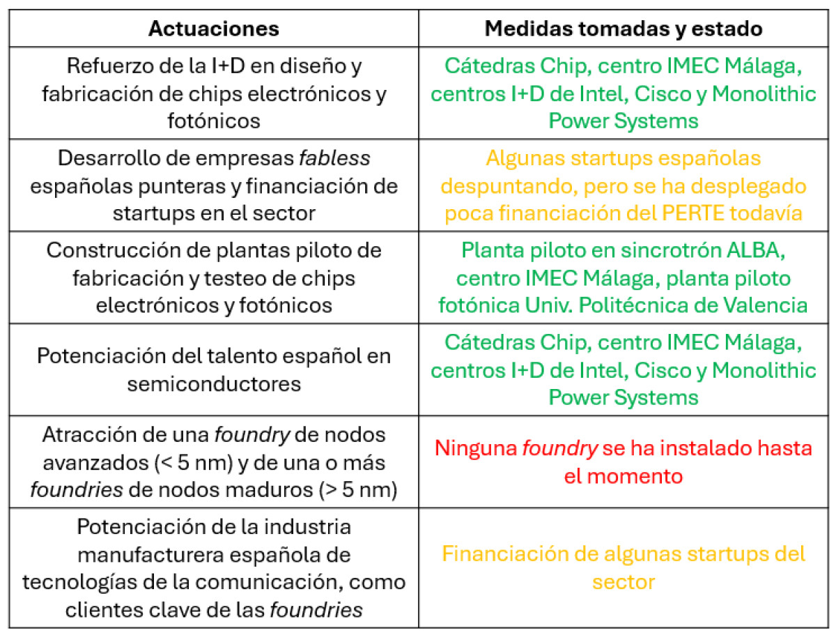
Fig. 2: Main actions contemplated in the PERTE Chip and the measures taken and achievements so far.
This is why, for example, TSMC is building six plants in the United States and eleven in its home country of Taiwan, but only one in Europe. And while the foundries in Taiwan and the United States focus on leading-edge nodes (dedicated to AI chips, the European foundry will work on 22 nm and 12 nm nodes, for industrial machinery and consumer microchips, such as those used in the automotive sector). The European project, in fact, is a TSMC joint venture with its main European customers: the project was not important enough on its own for TSMC to invest by itself.
“Although this PERTE Chip objective has been a failure so far, it has failed more due to its simple premise than to poor execution”
It is not surprising, therefore, that Spain has not managed to attract any chip production plants, especially given that the goal of attracting a foundry to produce logic chips at the 5 nm node or below was extremely ambitious, as can be seen by comparing with the nodes that the joint venture European of TSMC will produce. For these reasons, although this PERTE Chip objective has been a failure for now, it has failed more due to its simple premise — in retrospect, not very realistic — than due to poor execution.
On the other hand, the strategy for promoting R&D and talent in semiconductors is proving successful in its deployment. Funding through the PERTE of seventeen Chip Chairs at universities across the country will both boost national R&D in this field and significantly increase the talent pool in the medium term. Likewise, the establishment of chip design centers by Intel, Cisco and MPS in the Barcelona province will strengthen R&D and private-sector talent development across a wide range of chip typologies.
“The PERTE Chip is enabling constructions that will endow the Spanish semiconductor ecosystem with unique manufacturing and testing capabilities”
Regarding the creation of pilot plants for small-scale production and testing of next-generation microchips, the PERTE Chip is enabling the Innofab installation as part of the ALBA synchrotron in Barcelona, which will provide unique manufacturing and testing capabilities to the Spanish semiconductor ecosystem. In parallel, the Universitat Politècnica de València will build a pilot plant for photonic chips.
However, perhaps the greatest success (by far) of PERTE Chip so far is the announcement of the opening of an IMEC research center in Málaga. IMEC is the Belgian organization that leads global academic research in semiconductors across all areas: chip design and various applications, fabrication techniques, new materials, etc. IMEC also signs industrial research contracts with world giants and has created dozens and supported hundreds of semiconductor startups and related technologies in the last decade.
“IMEC Málaga will be the only major IMEC center operated outside its Belgian HQ, combining facilities for development, fabrication and testing of advanced chips with facilities for chip design”
That is why the establishment of this institution in Spain is so meaningful. IMEC Málaga will be the only large center operated by IMEC outside its Belgian headquarters, combining facilities for the development, fabrication and testing of advanced chips with others for chip design. Its presence in Málaga will not only create hundreds of highly qualified jobs, but in the medium and long term it will feed the sector with professionals in Spain’s semiconductor ecosystem and will generate a whole hub of companies and innovation around the south of Spain.
The way forward for Spain’s semiconductor strategy
Yet despite these successes, the shadow of failure to secure a foundry arrival in Spain weighs on the PERTE Chip’s overall success. Moreover, since the pillar of attracting foundries dominated PERTE’s funding and those funds were now uncommitted, they had to be redirected to the newly formed Sociedad Española para la Transformación Tecnológica (SETT).
SETT is responsible for deploying the remaining public funds of PERTE Chip and other initiatives —over 10,000 million euros more— to promote the creation of high value-added industries in Spain.
Through these funds, it has made significant investments in the semiconductor value chain and in consumer companies of advanced chips (Wallbox, Sensio, Sateliot).The broad geographic diversity of these investments also provides an important regional balance criterion and promotes industry nationwide. However, these investments are currently limited, and it remains to be seen how funds will continue to be allocated to companies.
“Failure has been marked by the high cost of these investments, intense international competition to attract them, and the lack of an attractive ecosystem in Spain”
So what can be said about the path ahead for SETT and Spain’s semiconductor strategy going forward? As has been noted, the failure to attract a major foundry to Spain has been driven by the high cost of these investments, the fierce international competition to attract them, and the lack of an attractive ecosystem in Spain in the field of advanced logic chips (which is the main focus of these foundries).
Based on this analysis, the Spanish strategy should focus on gaining capacity in areas where those problems do not arise, while building an ecosystem that addresses those shortcomings in the long term.
In this sense, PERTE Chip’s emphasis on photonics as a major opportunity for Spain is well aimed, since it is an emerging technology with relatively less international competition, that requires smaller investments (compared with a large foundry for electronics chips) and where Spain already has research centers (such as UPV, or the Universidad Politécnica de Vigo) and globally leading startups (iPronics, Mapsi Photonics, etc.).
Along these lines, the construction of the Valencia pilot plant, the SPARC photonic chip foundry investment, and the funding of several Chip Chairs focused on photonics are the first building blocks of Spain’s photonics industry, a well-identified opportunity by the PERTE Chip program.
On the other hand, it is surprising that the PERTE strategy did not emphasize attracting foundries for photonics signal and power electronics to Spain. Unlike logic chips, Spain does have experience (mainly around Valencia) and significant national customers (automotive, electronics for renewable energy, aerospace, etc.) that would purchase production from new national foundries.
“There have not been major investments in power electronics and signal chips to date, and it seems like a missed opportunity for the Spanish industry”
Moreover, the comparatively low costs of these foundries and the disruption brought by new advanced materials (GaN, SiC) versus traditional silicon offer an opportunity to gain market share and capacity in a key value chain for the ecological transition. But despite some initiatives funded by PERTE in this direction —such as the DioSiC industrial R&D project— there have not been major investments in power electronics and signal chips to date, and this seems a missed opportunity for the Spanish industry.
Another objective worth considering would be to attract encapsulation and testing plants for microchips, which perform the integration of chips into electronic devices (consumer goods, automotive, etc.) after production in a foundry. Our neighbor Portugal already hosts packaging plants, and the canceled Broadcom investment in Spain was going to be a packaging plant, which indicates the potential to attract such projects.
Regarding the dream of landing a foundry for logic chips, it would be prudent to combine modest short-term ambitions with a long-term development strategy. In the short term, the objective should be to install one or more foundries for chips in the 22 nm and larger nodes, which are mature nodes but dominate markets outside the leading foundries (TSMC, Samsung, and Intel).
“The global rise in demand for these chips and the relatively low cost of these kinds of foundries would also facilitate their arrival in Spain”
The global demand growth for these chips and the comparatively low costs of these types of foundries would likewise ease their entry into Spain. In the long term, together with the creation of leading fabless startups, this would also form a workforce that would be key to the future establishment of more advanced foundries.
In conclusion, the Spanish semiconductor strategy reflected in PERTE Chip is achieving some important successes, but so far it has failed to significantly raise national chip production. Reaching this strategic objective requires a strategic redirection with more pragmatic goals and a focus on areas (photonics, power electronics) where Spain can be a European and global leader.
